
Panel-Level Packaging: The Future of Advanced Semiconductor Packaging?

AmTECH Microelectronics
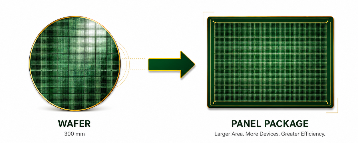
Panel-level packaging has become an increasingly important topic in advanced semiconductor packaging because it offers the potential for greater manufacturing area utilization, higher throughput, and lower cost per package. Wafer-level packaging, circular formatting, which is standard in the industry today, is not as productive as a panel because the edges of the wafer are mostly unusable. Wafer surface area is lost, and the argument is that rectangular panels are more easily utilized via panel, rectangular formatting.
Today, many products are being developed using technologies like wafer-to-wafer and chip-to-wafer technologies. In the future, there could be a rise in demand for chip-to-panel or panel-to-panel bonding. This is particularly substantiated by the fact that larger dies and silicon interposers are increasing in demand, currently by AI and hyperscale buildout.
One of the largest obstacles to broader panel-level packaging adoption is the semiconductor manufacturing infrastructure itself. Decades of investment have optimized equipment, automation, metrology, material handling, and process control around standardized wafer formats. Panel processing requires equipment capable of handling much larger rectangular substrates while maintaining the extremely tight tolerances required by advanced packaging. Subsequently, it would take a paradigm shift at every level of the ecosystem to move in the direction of panel-level packaging.
Key panel-level packaging challenges include:
- Panel warpage and substrate flatness
- Deposition uniformity
- Thermal expansion and CTE mismatch
- Defect inspection and metrology
- Material handling and automation
- Yield management
- Equipment interoperability
- Panel-size standardization
Panel-level packaging is currently most closely associated with fan-out technologies, although its potential extends beyond conventional fan-out packaging into RDL interposers, embedded-die technologies, advanced substrates, and glass-based packaging platforms.
Future panel-level packaging technologies could support:
- Fan-out panel-level packaging (FOPLP)
- RDL interposers
- Chiplet packaging
- Embedded-die packaging
- Advanced semiconductor substrates
- 2.5D semiconductor packaging
- Heterogeneous integration
- AI accelerator packaging
- High-bandwidth memory integration
- Large multi-chip modules
Rather than requiring the entire semiconductor ecosystem to abandon wafers, panel-level packaging is more likely to emerge as an additional manufacturing platform alongside wafer-based processes. If the industry can solve the remaining challenges surrounding yield, warpage, process uniformity and equipment standardization, panels could become particularly attractive for the increasingly large and complex advanced packages required by AI, high-performance computing and heterogeneous integration.